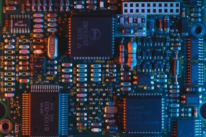
In the world of electronics, Printed Circuit Boards (PCBs) play a crucial role in ensuring the smooth functioning of various devices. Whether it’s a small electronic gadget or a complex industrial machine, PCBs are the backbone that connects and powers the components. When it comes to PCB manufacturing, JHDPCB has established itself as a leading provider of high-quality boards with exceptional precision and reliability. With a strong focus on innovation and customer satisfaction, JHDPCB offers an unparalleled experience in PCB production. One of the key areas where JHDPCB excels is in the manufacturing of PCB holes, which are vital for the proper functioning of the boards.
Understanding the Importance of PCB Holes
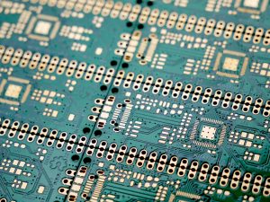
PCB holes are an integral part of the manufacturing process as they serve multiple purposes. These holes allow for the insertion of electronic components, such as resistors, capacitors, and integrated circuits, which are then soldered onto the board. They also facilitate the connection between different layers of the PCB through the use of vias, allowing for the flow of signals and power throughout the circuit. Properly drilled and positioned holes are essential for the overall performance and reliability of the PCB.
Types of Holes on PCBs
JHDPCB specializes in manufacturing different types of holes on PCBs to cater to a wide range of requirements. Let’s explore some of the common types of holes:
Plated Through-Holes (PTH): Plated through-holes are the most commonly used type of hole in PCBs. These holes have conductive material lining the walls, allowing for the passage of electrical signals and power between layers of the PCB. JHDPCB ensures precise drilling and plating of these holes, resulting in excellent conductivity and reliability.
Non-Plated Through-Holes (NPTH): Non-plated through-holes, as the name suggests, do not have conductive material lining the walls. These holes are primarily used for mechanical support or as mounting points for components that do not require electrical connectivity. JHDPCB provides accurate drilling and finishing for NPTH to meet specific design requirements.
Blind and Buried Holes: In some advanced PCB designs, blind and buried holes are used to create connections between specific layers without traversing the entire board. Blind holes connect an outer layer to one or more inner layers, while buried holes only connect the inner layers. These types of holes require precise manufacturing techniques, and JHDPCB has the expertise to deliver exceptional results.
Microvias: With the trend towards miniaturization, microvias have become increasingly popular in PCB manufacturing. These small-sized holes, typically less than 0.15mm in diameter, provide a high-density interconnection between layers. JHDPCB employs state-of-the-art equipment and techniques to achieve accurate and reliable microvia drilling.
The JHDPCB Advantage
When it comes to PCB manufacturing, JHDPCB stands out due to its commitment to excellence and customer satisfaction. Here are a few reasons why JHDPCB is the preferred choice for customers:
Advanced Technology and Equipment: JHDPCB continuously invests in advanced technology and equipment to ensure the highest level of precision and quality in PCB manufacturing. With state-of-the-art drilling and plating machines, they can meet the most demanding requirements.
Experienced Team: The team at JHDPCB consists of highly skilled and
experienced professionals who are passionate about their work. They have extensive knowledge of PCB manufacturing processes and are dedicated to delivering exceptional results.
Quality Assurance: JHDPCB has stringent quality control measures in place to ensure that every PCB meets the highest standards. From initial design review to final inspection, each board undergoes thorough testing and inspection to guarantee its reliability and functionality.
Timely Delivery: JHDPCB underst
ands the importance of timely delivery in today’s fast-paced industry. They have efficient production processes in place to meet deadlines without compromising on quality.
Annular ring pcb
When it comes to designing printed circuit boards (PCBs), the annular ring is a crucial element that requires careful consideration. An annular ring refers to the area of copper pad left between the edge of a drilled hole and the nearest copper trace or plane. To ensure proper functionality and reliability of your PCB, understanding the significance of the annular ring is essential. In this article, we will delve into the key aspects of annular ring PCB design and explore the factors that impact its integrity.
Conclusion
When it comes to PCB manufacturing, JHDPCB sets the bar high with its commitment to excellence, advanced technology, and experienced team. With a strong focus on providing high-quality PCB holes, JHDPCB ensures that every board meets the stringent requirements of the industry. Whether it’s plated through-holes, non-plated through-holes, blind and buried holes, or microvias, JHDPCB delivers precision, reliability, and unmatched customer satisfaction. Experience excellence in PCB manufacturing with JHDPCB and witness the difference it can make in your electronic devices.
